Having read about old mainframe magnetic core ROM, I decided to try and build my own. I conducted a few experiments with some parts I had, and it surprisingly looked like it would work.
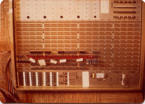
I acquired some surplus pulse transformers, and broke off the epoxy potting away to get the ferrite core. I used 32 cores for 32-bit-wide storage. With 8 drivers on the top and 8 switches on the bottom I could support 64 lines, for 256 bytes of storage (although I planned for 1024 bytes). As I recall, 256 bytes was enough to handle some basic keyboard functions, the teletype, and the tape.
The breadboard was just a surplus wire-wrap board I got for a good price because it was fully wired and used. In the end, removing the wires and getting punctured by wire-wrap pins was such a pain that I snapped off all the pins and just soldered to the stumps.
Each line was hand-threaded through the appropriate cores to produce a '1'; non-threaded cores produced a '0'. The magnetic-core ROM worked very reliably; better, in fact, than I could possibly have hoped.
On the same board I eventually added an external hardware stack, using 7489 devices and port input/output instructions. In the 8008, sometimes one simply could not move a value from one register to another, and the stack supported general movement.
Eventually I was able to buy a 1702 EROM programmer board, although it was really just a half a board cut from something else which had a programmer on it. But I was able to build that up and make it work under 8008 control. I made an EROM eraser from an old UV sanitation bulb with a regular light bulb as a ballast. Then I got a Mark-8 memory board for the 1702's, which greatly expanded my ROM limits, and I eventually decommissioned the magnetic core ROM. The wires remain, but the driver transistors are gone.
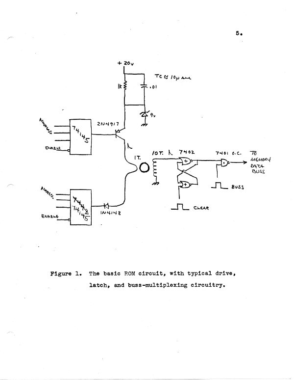
Basically a report for credit in a Digital Logic course, it describes the magnetic ROM design:
The first design.
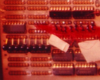
At the left we see eight PNP driver transistors. Each transistor drives up to eight lines.
The transistors are directly driven from a TTL multiplexer. This was "active LOW," so only one transistor base was grounded at a time. Current was limited by the energy stored in the pulse capacitor on the back. This was connected through a resistor to Vcc.
Just up and to the right we can see the first eight cores, the fuzzy black things that appear to be wiggling around. The drive lines themselves are hard to see because they are very thin wires in light orange enamel, although one line can be seen against the tape background.
Each core had a winding that connected to a TTL NOR gate. Two of the four gates in a package were wired as a latch for a single core. Before the pulse was sent, all latches were cleared. If the selected line ran through a particular core, the current pulse was enough to set the associated latch
The drafting tape flags probably indicated the start
or end of different sections of code.
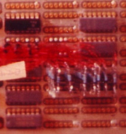
Here we see the last four cores and the lines connecting to the individual diodes.
At the right we see eight stacks of eight diodes each. Each line had a diode to prevent currents from sneaking back through the supposedly "off" lines.
Each diode stack connected to one output of a TTL multiplexer. This was "active LOW" so only only one bank was grounded at a time.
With a selection on the top, and a selection on the bottom, only one line got a current pulse. If the selected line ran through a particular core, the current pulse was enough to set the associated latch
After the latches were set, the appropriate byte (of four)
was selected and gated onto the data bus.
Last updated: 2002 Feb 21